HES-DVM 
HARDWARE ASSISTED VERIFICATION / HW-V / PROTO / ASIC
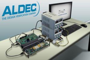
HES-DVM is Aldec’s fully automated verification and validation system for SoC and ASIC designs of 600M+ gates. This Hardware Emulation Solution is based on the latest Xilinx Virtex-7 and UltraScale devices and is capable of simulation acceleration, and SCE-MI transaction co-emulation.
RTL Debug
HES-DVM provides full control of the system in both acceleration and co-emulation with SCE-MI. As well as control, HES-DVM provides 100% design visibility and with Aldec’s HVD technology the impact on system performance can be minimised. HES-DVM also includes Aldec’s SyntHESer high-speed HDL synthesizer, which performs 10x faster than a leading standalone synthesis tool.
Debug Capabilities
- High performance debug infrastructure (HMDB bus)
- Flexible static probes, advanced embedded logic analyser for at-speed RTL debug
- Dynamic debugging with HVD technology
- Emulation triggering and control capabilities
- Memory viewer and write access tools including API
Hybrid Virtual Prototyping
Utilising virtual platforms with HES-DVM’s co-emulation interface, developers are able to connect SystemC TLM 2.0 modules to their hardware DUT via high speed transactors. HES-DVM memory management API enables developers to load applications to program memory, decreasing overall system boot-time.
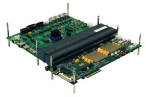
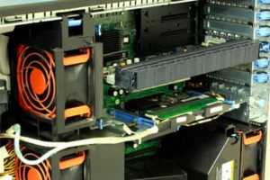
HES A Scalable System
The use of Xilinx devices is a cost-effective solution for hardware emulation and enables replication of the system for software development and verification regression systems. Aldec supports customer FPGA systems as part of its custom board support.
Time To Emulation / TTE
The use of Xilinx devices is a cost-effective solution for hardware emulation and enables replication of the system for software development and verification regression systems. Aldec supports customer FPGA systems as part of its custom board support.
 David Clift, Applications Specialist, FirstEDA