Ian Gibbins
FirstEDA

Ian Gibbins
FirstEDA
Here is a reminder that we shouldn’t take technology for granted!
—
I recently moved to a new house, having spent 25 years putting down roots following a somewhat nomadic earlier life.
Among the many daunting tasks laid before me was 25 years of accumulated boxes in the loft … and it was a big loft!
While sorting through the menagerie of ‘stuff’, I came across some old logbooks back from my days as an apprentice. At just 17, I was lucky enough to be placed in the VLSI department at Standard Telecommunication Laboratories, a highly regarded research establishment. I recall arriving in the department and seeing a chip plot of one of the first analogue pagers on the wall. It looked like a futuristic street map, and I instantly knew I had to know everything about VLSI!
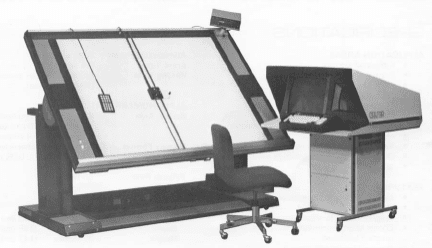
With a vociferous appetite to learn and surrounded by brilliant colleagues, I quickly came up to speed with SPICE models, silicon processes and the design rules that allowed these fantastic collections of transistors to perform a predictable function. I ultimately became a key member of the design team, supporting SPICE simulations and working in the CALMA room (Figure 1). This was the NASA Space Centre’s equivalent back then, as far as I was concerned!

Figure 1: CALMA digitiser workstation
After carefully digitising each layer based upon the SPICE netlist and the process rules, the layout team finished the 10,000-transistor landscape, or so I naively thought. In my early days in the VLSI department, I had often wondered what some of the engineers were doing in a large empty room, on their hands and knees poring over large plots and computer printouts with a ruler in one hand and a pencil in the other. Soon enough, I learned that this was how to ensure that the layout matched the SPICE netlist; this was Design Rule Checking!
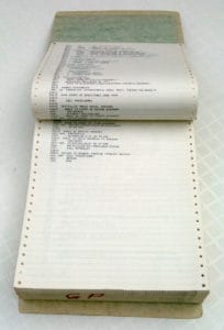
It was soon my turn to monitor the plotting from a huge electrostatic plotter (Figure 2) and carefully transport several rolls to the checking room. A colleague (and still a very good friend to this day) would bring the very thick printout of the whole chip SPICE netlist (Figure 3), and with our pencils and rulers, we would embark.

Figure 2: Colour electrostatic plotter
One of us would begin on the first line of the SPICE netlist, while the other located the equivalent position on the chip plot. One would measure the drain, source and gate of that transistor to ensure it matched the netlist, then move on to where each part was connected, tracing with a pencil. We would regularly swap roles since the chip plot measuring and tracing became wearing on the knees and back after a while! We would dream of a day when someone could automate this process, and whilst we indeed had colleagues developing DRC and LVS programs, we endured this process for several designs.

Figure 3: SPICE netlist printout of whole chip
Some five years later, I worked with another company alongside the same colleague on Wafer Scale Integration products.
Our earlier conversations of design automation were a new reality, with design rule checking and layout extraction tools available. However, it required a lot of work on our part to build the checker rulesets. I was so eager to prove this early technology and spent many long days (and nights) building and testing to make it work to benefit all the colleagues using the design flow. Some of them could not understand my tenacity and drive and, looking at the knees of their trousers and lack of decent pencils and rulers, I knew why!
When I look back at my years spent in design automation, it is the early years of developing technology that impresses me the most for the simple reason that verification was a lot of hard work. There were no tools to help in the verification process (pencils and rulers aside). I was enthusiastic about embracing new tools that could assist the verification process and was aware that as time moved on and design automation became pervasive, we began to take it for granted.
Today, there is so much automation that allows for much more complexity, and such complexity still requires verification. Verification should begin as early as possible, which means at the language level. There are language design entry tools such as Sigasi, a sophisticated code editor with an underlying compiler technology that checks code as it is typed, giving instant feedback on errors and potential issues – all pre-simulation.
Sigasi also has an interface to Aldec’s ALINT-PRO, which emulates coding reviews in a short space of time. It achieves this with a combination of fast synthesis technology and design rule policies. This Design Rule Checking (or linting as it is historically known) is a static HDL code analysis process that can uncover bugs hidden in the code.
Choosing tools for early design analysis in a methodology can address the debugging phase’s uncertainty during verification. Such tools can likely automate the discovery of up to 80% of typical RTL coding mistakes during the early design stages. Finding these issues so early can save many hours on hands and knees with pencils and rulers (metaphorically speaking) later in the design phase. This is great news as chances are if I resorted to the manual approach today, I wouldn’t be able to get back up!
If you would like to discuss design verification tools such as Sigasi or Riviera-PRO, then please contact us.