HES 
PROTOTYPING BOARDS / HW-V / PROTO / ASIC
HES provides SoC and ASIC verification and validation teams with a scalable and high-quality FPGA-based ASIC prototyping solution.
HES is a SoC/ASIC pre-silicon prototyping solution for hardware verification and software validation teams and a High Performance Computing (HPC) platform for algorithms acceleration. The boards are based on largest Virtex-7 and Virtex UltraScale FPGA and appear in single or multi-FPGA configurations and can be interconnected on a backplane board providing up to 663 Million ASIC gates.
VIRTEX ULTRASCALE+ BOARDS
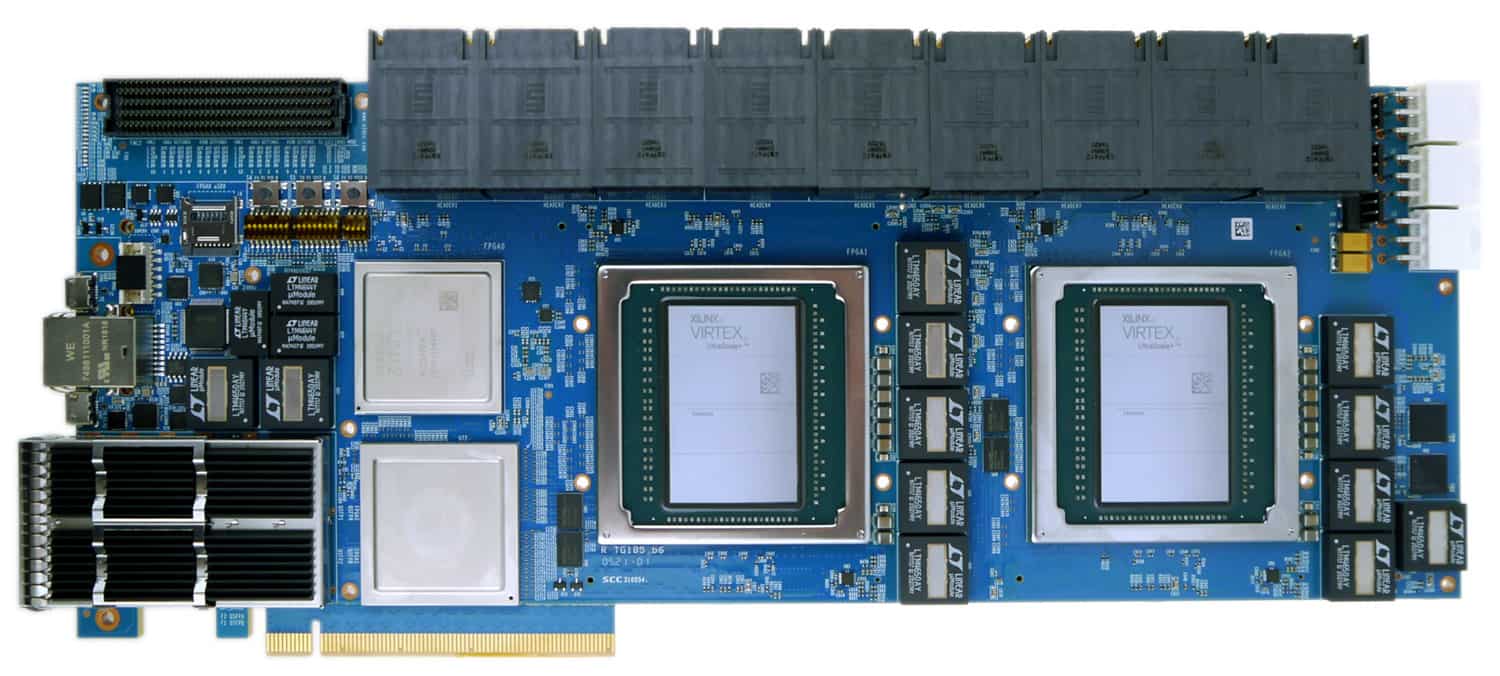 HES-VU19PD-ZU7EV
The HES-VU19PD-ZU7EV offers a unique combination of two Virtex UltraScale+ VU19P FPGAs as logic module and one Xilinx Zynq UltraScale+ ZU7EV MPSoC as the host module that features a Quad-core ARM® Cortex-A53, Dual-core ARM® Cortex-R5 real-time processing units, an ARM® Mali-400 MP2 GPU, integrated H.264/H.265 video codec, and UltraScale+™ programmable logic in a 16nm FinFET node. Read more..
 HES-XCVU9P-QDR
HES-XCVU9P-QDR contains a Virtex UltraScale+ XCVU9P FPGA with dual QSFP28 cages for high-bandwidth low-latency communications. Onboard QDR-II+ or DDR4 memory provides ultra-fast data rate transfers for applications requiring high throughput. The PCIe x16 half-length low-profile board enables maximum performance density in any enterprise rack server system. Read more..
 HES-XCVU9P-ZU7EV
HES-XCVU9P-ZU7EV contains a Zynq UltraScale+ ZU7EV MPSoC with Virtex UltraScale+ XCVU9P FPGA for high-performance compute-intensive applications. The ARM computing platform on the Zynq device combined with UltraScale+ programmable logic allows for high-speed processing and ultimate custom designability in a standard PCIe 3.0 x16 form factor. Read more..
VIRTEX ULTRASCALE BOARDS
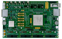 HES-US-440
HES-US-440 contains one XCVU440 logic module and Xilinx Zynq-7000 host module featuring ARM dual core Cortex-A9 CPU. This board has been optimized for high speed physical prototyping and emulation of medium size ASIC designs up to 26 Million gates. Unique combination of large capacity UltraScale FPGA and Zynq-7000 SoC allows to build a self contained single board testbench for your design. Read more..
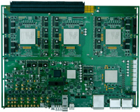 HES-US-1320
HES-US-1320 with three XCVU440 logic modules is Aldec’s large capacity FPGA board targeted to high speed physical prototyping and emulation of ASIC and SoC designs. The board provides estimated capacity of 79 Million gates, supports up to 48 GB DDR4 in six SO-DIMM slots and it is easily extendable with non-proprietary connectors (BPX & FMC). Read more..
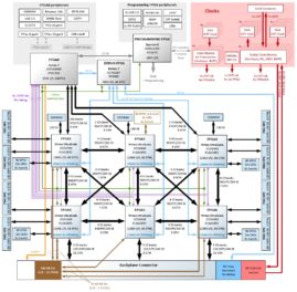 HES-US-2640
HES-US-2640 with six XCVU440 logic modules is Aldec’s largest capacity FPGA board targeted to high speed physical prototyping and emulation of ASIC and SoC designs. The board provides estimated capacity of 158 Million gates, supports up to 48 GB DDR4 in six SO-DIMM slots and it is easily extendable with non-proprietary connectors (BPX & FMC). Read more..
VIRTEX-7 BOARDS
 HES7XV4000BP & HES7XV1380BP
HES7XV4000BP and HES7XV1380BP are dual FPGA prototyping and emulation boards for small-medium size ASIC designs or large FPGA designs. The board is available in two configurations with Virtex-7 2000T or 690T FPGA. The HES7XV4000BP estimated capacity is 24 Million ASIC gates and is easily extendable via non-proprietary connector (BPX). Read more..
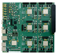 HES7XV12000BP
HES7XV12000BP with six Virtex-7 2000T logic modules is Aldec’s large capacity FPGA board targeted to high speed physical prototyping and emulation of ASIC and SoC designs. The board provides estimated capacity of 72 Million gates and is easily extendable via non-proprietary connectors (BPX and FMC). Read more..
HES BACKPLANE BOARDS
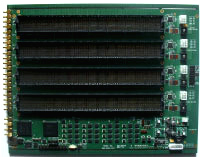 HES7BPX4
HES7BPX4 is a backplane board used to build hardware platforms larger than single HES-US or HES-7 FPGA Main board. The largest configuration can provide up to 633 Million ASIC gates. It is build of MOLEX connectors mated with HES Main FPGA boards to provide passive, cross board I/O interconnections. Careful design of clock distribution tree assures configurability and flexibility. The JTAG chain from all main boards are integrated on backplane board and provide a common FPGA programming port for all FPGA logic modules in the system. Read more..





 David Clift, Applications Specialist, FirstEDA