Farhad Fallahlalehzari
ALDEC

Farhad Fallahlalehzari
ALDEC
Faster inference in DNN-based applications using FPGAs
—
Machine learning is the process of using algorithms to parse data, learn from it, and then make a decision or prediction. Instead of preparing program codes to accomplish a task, the machine is ‘trained’ using large volumes of data and algorithms to perform the task on its own.
Machine learning is being revolutionised using neural network (NN) algorithms, which are digital models of the biological neurons found in our brains. These models contain layers which are connected like a brain’s neurons. Many applications benefit from machine learning, including image classification/recognition, big data pattern detection, ADAS, fraud detection, food quality assurance and financial forecasting.
As algorithms for machine learning, neural networks include a wide range of topologies and sizes consisting of multiple layers; the first layer (a.k.a. input layer), middle layers (a.k.a. hidden layers) and the last layer (a.k.a. output layer). Hidden layers perform a variety of dedicated tasks on the input and pass it to the next layer until, at the output layer, a prediction is generated.
Some neural networks are relatively simple and have only two or three layers of neurons, while so-called Deep Neural Networks (DNNs) might comprise up to 100/1000 layers. Determining the right topology and the size of the NN for a specific task requires experimentation and comparison against similar networks.
Designing a high-performance machine learning application requires network optimisation, which is typically done using pruning and quantizing techniques, and computation acceleration, which is performed using ASICs or FPGAs [1].
In this article, we will discuss how DNNs work, why FPGAs are becoming popular for DNN inference and consider the tools you need to start designing and implementing a deep learning-based application using FPGAs on Aldec’s TySOM-3A-ZU19EG Embedded Development Board which has the largest FPGA in Xilinx Zynq US+ MPSoC family.
Design flow for developing a DNN application
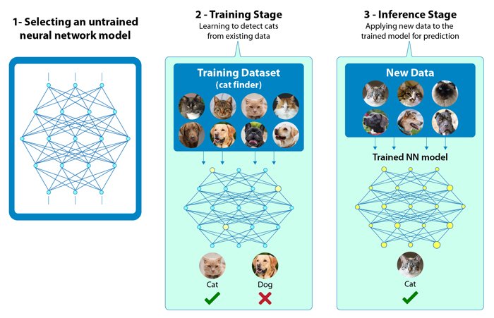
Designing a DNN application is a three-step process. The steps are choosing the right network, training the network and then applying new data to the trained model for prediction (inference). Figure 1 illustrates the steps for an application to recognise cats.

Figure 1 – The three steps of recognising a cat.
As mentioned, there are multiple layers in a DNN model, and each layer has a specific task. In deep learning, each layer is designed to extract features at different levels. For example, in an edge detection neural network, the first middle layer detects features such as edges and curves. The output of the first middle layer is then fed to the second layer, which is responsible for detecting higher level features, such as semicircles or squares. The third middle layer assembles the output of the other layers to create familiar objects and the last layer detects the object.
In another example, if we set out to recognise a stop sign, the trained system would include layers for detecting the octanol shape, the colour and the letters S, T, O, and P in that order and in isolation. The output layer would be responsible for determining if it is a stop sign.
DNN learning models
There are four main learning models:
Training vs inference
In training, the untrained neural network model learns a new capability from the existing data. Once the trained model is ready, it is fed new data and the performance of the system is measured. The ratio of detecting the image correctly is called inference.
In the example given in figure 1 (recognising a cat), after inputting the training dataset the DNN starts tuning the weights to find cats; where a weight is a measure of the strength of the connection between each neuron.
If the result is wrong, the error will be propagated back to the network’s layer to modify the weights. This process happens again and again until it gets the correct weighting, which results in getting a correct answer every time.
How to achieve a high-performance DNN application
Using DNN for classification requires a big dataset, which increases the accuracy. However, a drawback is that it produces many parameters for the model, which increases the compute cost and requires high memory bandwidth.
There are two main ways to optimise a DNN application. The first is network optimisation through pruning redundant connections and quantizing the weights and fusing the neural networks to narrow down the network size.
The second way to optimise the DNN is through computation acceleration, using ASICs or FPGAs. Of these, the latter option has many benefits for machine learning applications. Comparison between GPUs and FPGAs are elaborately studied in another article “FPGA vs GPU for Machine Learning Applications: Which one is better?” Here are some of the highlights
Modern FPGAs typically offer a rich set of DSP and BRAM resources within their fabric that can be used for processing NN. However, compared to the depth and layer size of DNNs, these resources are no longer enough for a full and direct mapping; certainly not in the way it was often done in previous generations of neural network accelerators. Even using devices like the Zynq MPSoC, where even the largest device is limited to 2k DSP slices and a total BRAM size of less than 10MB, a complete mapping with all neurons and weights directly onto the FPGA is not possible.
So, how can we use the power efficiency, re-programmability, low latency and other features of FPGAs for deep learning?
New NN algorithms and architectural modification are required to enable the inference of DNNs on platforms with limited memory resources such as FPGAs.
A modern DNN divides the applications into smaller chunks to be processed by FPGAs. Since the on-chip memory in FPGAs is not enough for storing all the required weights for a network, we have to store only the weights and parameters for the current stage which are loaded from an external memory (which could be a DDR memory).
However, transferring data back and forth between the FPGA and memory is going to increase the latency up to 50 times. The first thing that springs to mind is to reduce the memory data. In addition to the network optimisation discussed above (pruning and quantization), there are:
Design and Implementation of DNN applications on FPGAs
Let us now dive into implementing a DNN in FPGAs; and it makes sense to take full advantage of the most appropriate commercially available solutions to fast-track the development of an application.
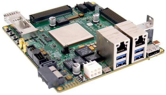
For instance, Aldec has an embedded development board called the TySOM-3A-ZU19EG. This board carries the device which carries the largest FPGA in the Xilinx Zynq UltraScale+ MPSoC family (ZU19EG), which includes a quad-core ARM Cortex-A53 platform running up to 1.5GHz, along with a wide range of peripherals such as QSFP+, mPCIe, SATA, USB 3.0, HDMI 2.0. Xilinx has developed a deep learning processing unit (DPU) for machine learning developers that is supported on the Zynq MPSoC devices. Using Aldec TySOM boards we can develop DNN applications using Xilinx DPU. Figure 2 shows TySOM-3A-ZU19EG embedded development board.

Figure 2 – TySOM-3A-ZU19EG Embedded Development Board
Importantly, for our purposes, this mammoth MPSoC also supports Xilinx’s deep learning processing unit (DPU), which the company created for machine learning developers.
DPU and DNNDK
The DPU is a programmable engine dedicated for convolutional neural networks. It is designed to accelerate the computing workloads of DNN algorithms used in computer vision applications such as image/video classification and object tracking/detection etc.
There is a specific instruction set for DPU, which enables a DPU to work efficiently for many convolutional neural networks. Like a regular processor, a DPU fetches, decodes and executes instructions stored in DDR memory. This unit supports multiple CNNs such as VGG, ResNet, GoogLeNet, YOLO, SSD, MobileNet, FPN, etc [3].
The DPU IP can be integrated as a block in the programmable logic (PL) of the selected Zynq-7000 SoC and Zynq UltraScale+ MPSoC devices with direct connections to the processing system (PS).
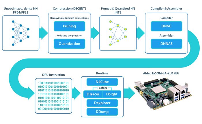
To create the instructions for DPU, Xilinx provides a Deep Neural Network Development Kit (DNNDK) tool kit. Xilinx states: “The DNNDK is designed as an integrated framework, which aims to simplify and accelerate deep learning application development and deployment on the Deep Learning Processor Unit (DPU). DNNDK is an optimising inference engine, and it makes the computing power of DPU become easily accessible. It offers the best of simplicity and productivity to develop deep learning applications, covers the phases of neural network model compression, programming, compilation, and runtime enablement” [4].
The DNNDK framework comprises the following units:

Figure 3- The Above Deep Neural Network Development Kit (DNNK) framework makes the design process of an FPGA-based machine learning project much easier for developers.
Using DNNDK makes the process of designing an FPGA-based machine learning project much easier for developers; In addition, platforms like the afore-mentioned Aldec’s TySOM-3A-ZU19EG board are also there to provide an invaluable kick-start. For instance, Aldec has prepared some examples – including gesture detection, pedestrian detection, segmentation and traffic detection – that target the board, meaning developers are not starting with a blank sheet.
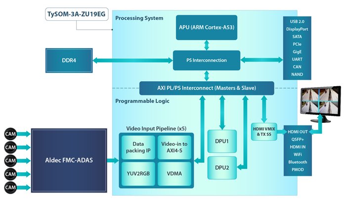
Let us consider one now, one that was showcased at Arm TechCon earlier this year. It was a traffic-detection demonstration, built using a TySOM-3A-ZU19EG and an FMC-ADAS daughter card; which provides interfaces and peripherals for 5x HSD cameras, RADAR, LIDAR and ultrasonic sensors – i.e. sensory inputs for most ADAS applications.
Figure 3 shows the architecture of the demo. There are two DPUs implemented to FPGA which are connected to the processing unit using AXI HP ports to perform deep learning inference tasks such as image classification, object detection and semantic segmentation. The DPUs require instructions to implement a neural network which are prepared by DNNC and DNNAS tools. They also need access to memory locations for input videos as well as output data.
An application is run on the Application Processing Unit (APU) to control the system by managing interrupts and performs data transfer between units. The connection between the DPU and the user application is by DPU API and Linux driver. There are functions to read a new image/video to DPU, run the processing and send the output back to the user application.

Figure 4 – Above, the traffic-detection demo has 5x video input pipelines that are used for data packing, AXI4 to AXI Stream data transferring, colour space conversion (YUV2RGB) and sending the videos to memory.
Developing and training the model is done using Convolutional Architecture for Fast Feature Embedding (Caffe) outside of the FPGA, whereas optimisation and compilation is done using DECENT and DNNC units provided as a part of the DNNDK tool kit (figure 2). In this design, the SSD object detection CNN is used for background, pedestrian and vehicle detection. You can read more info about this solution on “Deep Learning Using Zynq US+ FPGA”.
In terms of performance, up to 45 fps was achieved – which is an improvement in the efficiency of a traffic detection system. For future projects, we are preparing a traffic sign detection using DNN on TySOM-3A-Zu19EG board.
References
[1] Guo, Kaiyuan, et al. “A survey of fpga-based neural network accelerator”
[2] FPGA-based Accelerators of Deep Learning Networks for Learning and Classification: A Review
[3] DPU for convolutional neural network “Xilinx.com”
[4] DNNDK user guide “Xilinx.com”
[5] Efficient deep neural network acceleration through FPGA-based batch processing