Igor Tsapenko
ALDEC Director, Applications Engineering

Igor Tsapenko
ALDEC Director, Applications Engineering
The multi-channel parallelism and low-latency access of NAND flash technology have made Non-Volatile Memory express (NVMe) based SSDs very popular within the main segments of the data storage market
—
Including not only the consumer electronics sector but also data center processing and acceleration services, where the key role is played by specialised FPGA-based hardware for application-specific workloads.
Aldec has risen to the increasing demand for NVMe connectivity solutions for FPGA-based emulation and prototyping platforms by extending its portfolio of FMC-based I/O expansion daughter cards to include stackable FMC-NVMe boards and offering support for x4 NVMe SSDs in M.2 form factor via high-performance PCIe switch.
The easiest way to verify the performance of this FMC-NVMe card is to connect one to a TySOM-3 or 3A board from Aldec’s Zynq US+ MPSoC-based embedded prototyping board product line. These boards are capable of interfacing with NVMe thanks to an integrated PCIe block located in Programmable Logic (PL) part of the MPSoC and under the control of the embedded Linux running on the ARM Cortex-A53 cores in the Processing System (PS) part of the MPSoC.
In this blog we shall evaluate the performance potential of Aldec’s TySOM-NVMe bundle in real world benchmarking tasks and highlight the details of reference designs that are available for all customers to reduce their system bring-up time and to simplify their customisation efforts.
Hardware Design in Xilinx Vivado
Provided the FMC-NVMe acts as a PCIe Endpoint device, and because the NVMe protocol requires 4x PCIe Gen3 lanes, the hardware design for the Zynq US+ MPSoC host is focused on PCIe Root Complex subsystem implementation.
The Root Port of PCIe Root Complex is built over the high-performance and configurable Xilinx AXI Bridge for PCIe Express Gen3 IP (XDMA), which is based on the PCIe Gen3 integrated block available in UltraScale+ FPGA devices. The overall block design from Vivado IP Integrator is shown in Figure 1 (Vivado 2018.3).

Figure 1: PCIe Root Complex Host Implementation (TySOM-3-ZU7EV)
The PCIe Root Complex is connected by x8 Gen3 lanes to the 32-lane Microsemi PM8532 PCIe switch available on the FMC-NVMe daughter card via high-pin count (HPC) FMC connector (FMC1), which yields 64 Gb/s of theoretical bandwidth. The main PCIe configuration parameters are shown in Figure 2.
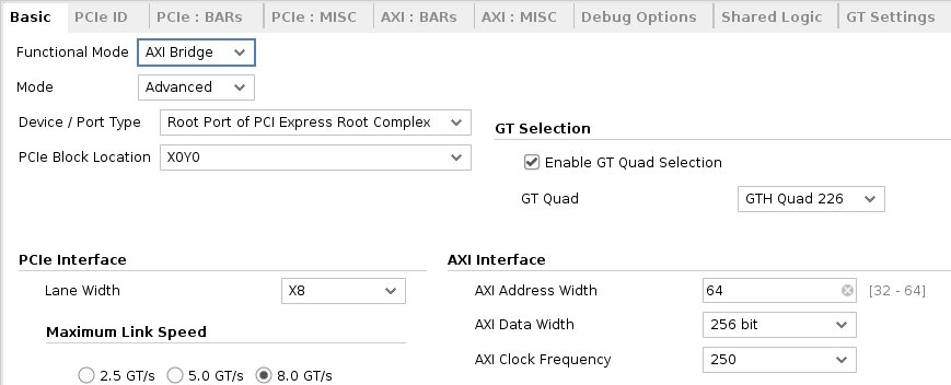
Figure 2: PCIe Bridge Basic Parameters (TySOM-3-ZU7EV)
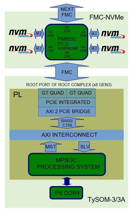
Note, the FMC1 connector provides the required 8x GTH links between the MPSoC host and the FMC-NVMe for both TySOM-3-ZU7EV and TySOM-3A-ZU19EG boards. The PM8532 switch is responsible for interfacing with 4x NVMe SSDs connected to the 4-lane M.2 connectors. The remaining 8 lanes are routed to the top FMC connector for the upstream FMC-NVMe card in a stack. The overall system topology is shown in Figure 3.
Although the referenced PCIe Root Complex subsystem implementation is general-purpose and can work with most kinds of PCIe endpoint device, there are several system design considerations that have been taken into account, especially for NVMe SSDs support, to guarantee the seamless interoperability of hardware, IP and the corresponding Linux driver (pcie-xdma-pl).
These considerations are:
Please refer to the Xilinx Answer Record 70854 document for a full list of MPSoC PCIe Root Complex PL implementation tips.
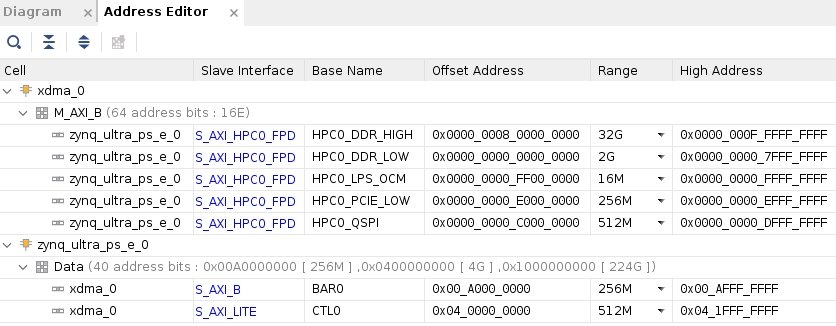
Figure 4: Address Mapping for XDMA IP
NVMe Support in Linux
During recent years, several major enhancements have been integrated into the mainline kernel to support the NVMe protocol, including not only the nvme driver itself but also several improvements in the block layer for efficient block I/O requests processing.
The embedded Linux kernel used in our reference design is built from Xilinx’ kernel source tree (v2018.3 – 4.14.0 kernel version) from xilinx_zynqmp_defconfig default configuration file for arm64-based Zynq US+ MPSoC devices. Note, support for MPSoC PL-based PCIe Root Complex and NVMe block layer is disabled by default and two additional drivers must be manually selected, as shown in figures 5 and 6.

Figure 5: Selecting XDMA PCIe Host Driver
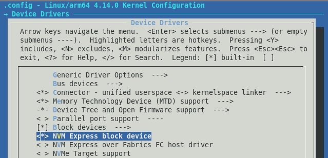
Figure 6: Selecting NVMe Block Device Driver
NVMe Userspace Benchmarks
The reference solution was tested with different models of NVMe SSDs in the M.2 form factor. These included the top-selling cards from Western Digital and Samsung as well as cost-optimised (Lite-On) ones. The complete up-and-running hardware setup based on TySOM-3A-ZU19EG board with x1 FMC-NVMe and x4 NVMe SSD storages connected is shown in Figure 7.
The main idea of performing the benchmarks was to measure the linear read/write data rates achievable with TySOM-NVMe bundle and to compare them to the ones declared by NVMe drive manufacturers.
After successful Linux OS boot-up, the next step is to verify the presence of the connected NVMe SSDs in system that can be easily done with nvme-cli tool (shown in Figure 8), which is the main tool for NVMe management in Linux userspace.
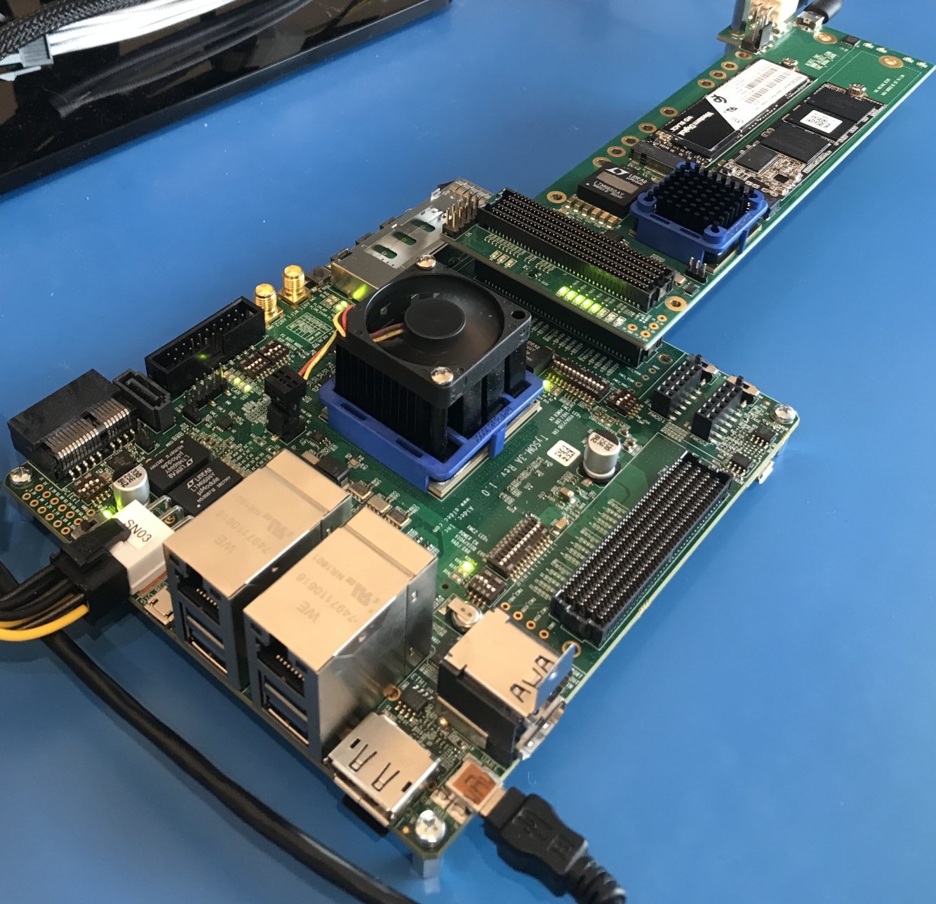
Figure 7: Complete HW Setup Based on TySOM

Figure 8: NVMe SSDs Discovered by nvme-cli Tool
Linear I/O estimations were made using the standard dd command line utility. Note, the DIRECT_IO approach was used to avoid some Linux VFS stack overhead, such as Page Cache translations for paged data blocks, to submit I/O requests directly to Block I/O Layer and then to nvme hardware driver.
More detailed monitoring of read/write operations trace through Linux kernel stack can be done with Perf performance analysis and profiling userspace command line utility. The simplified function call trace caught by Perf is shown in Figure 9.
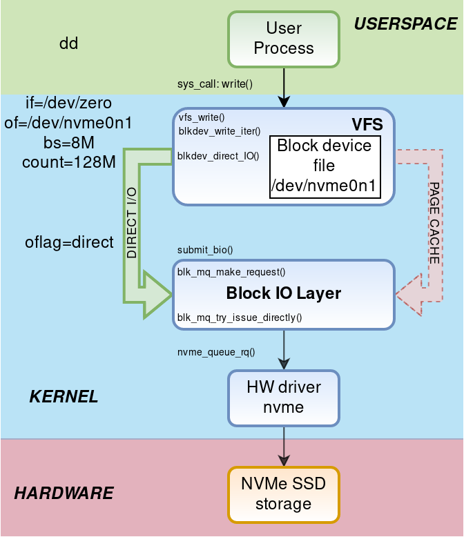
Figure 9: Simplified Kernel Trace for Issued Write Operations
The benchmark results show an approximately linear dependency between data transfer speed and data transfer size, with its peak value at 3.3 GB/s for read. In the case of write transfers, each tested NVMe SSD has its own area of peak performance (1.0 to 1.5 GB/s) due to the different sizes of high-speed SLC NAND memory implemented as write cache, when the most of the data storage is made using slower TLC NAND technology.
Figure 10 clearly shows that this level of NVMe I/O performance is unreachable using standard Page Cache mechanism, which delivers about 3x slower data rates (850 MB/s RD and 550 MB/s WR).
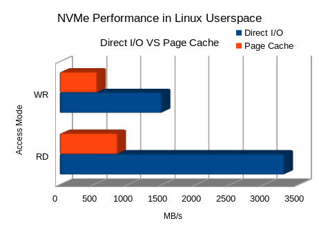
Figure 10: Direct I/Os vs. Page Cache Data Rates
A comparison of collected performance data against declared values is shown in figures 11 and 12 for read and write operations respectively.
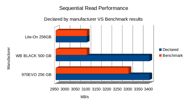
Figure 11: Read Performance Comparison
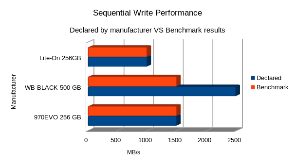
Figure 12: Write Performance Comparison
As can be seen, TySOM-NVMe interfacing solution’s performance was good enough to squeeze the max out of cost-optimised NVMe SSDs delivering 3100 MB/s for read and 1000 MB/s for write; as claimed by the vendor.
In the case of storage drives with higher I/O performance, the acquired data rates go higher too, almost reaching the top values for the NVMe drives used in the tests.
Last, but not least, the I/O operations can be performed on several storage drives simultaneously to get even higher overall data transfer rates. During the current benchmarks, the peak performance for simultaneous 4x drives I/O interfacing was limited by 4 GB/s for read and about 3.4 GB/s for write.
Conclusion
Aldec’s TySOM-NVMe hardware bundle proved to be a great demonstration of multi-gigabit per second NVMe SSD performance that can be achieved with this class of embedded platform.
Despite the availability of custom proprietary NVMe IP accelerators from the IP design companies on the market, the embedded MPSoC-based solution provided sufficient data transfer rates and feature-richness which, along with the flexibility of the Linux OS, can satisfy the continuously growing I/O speed rate needed for a broad range of specialised data storage applications.